|
| Brand Name: | Winsmart |
| Model Number: | SMTL460 |
| MOQ: | 1 set |
| Price: | USD1-150K/set |
| Packaging Details: | Plywood case |
| Payment Terms: | L/C, T/T, Western Union |
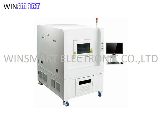
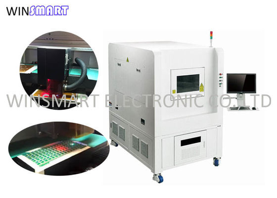
CCD Camera PCB Laser Depaneling Machine PCB Laser Depanelizer
Typical UV Laser Applications:
1. Depaneling flex and rigid PCBs
2. Cover layer cutting
3. Cutting fired and unfired ceramics
4. Microvia drilling
5. Skiving (cover layer removal)
6. Pocket creation
Advantages of Laser Technology:
Compared to conventional tools, laser processing offers a compelling series of advantages.
1. The laser process is completely software-controlled. Varying materials or cutting contours are easily taken into account by adapting the processing parameters and laser paths. There is also no need to factor in retooling times during a change of production.
2. No appreciable mechanical or thermal stresses occur. The ablation products are extracted by suction directly at the cutting channel. Even sensitive substrates can thus be precisely processed.
3. The laser beam merely requires a few µm as a cutting channel. More components can thus be placed on a panel.
4. The system software differentiates between production and set up processes which drastically reduces instances of faulty operation.
Specification:
| Laser | Q-Switched diode-pumped all solid-state UV laser |
| Laser Wavelength | 355nm |
| Laser Source | Optowave UV 15W@30KHz |
| Positioning Precision of Worktable of Linear Motor | ±2μm |
| Repetition Precision of Worktable of Linear Motor | ±1μm |
| Effective Working Field | 460mmx460mm(Customizable) |
| Scanning Speed | 2500mm/s (max) |
| Working field | 40mmх40mm |
Production:
![]()
|
|
| Brand Name: | Winsmart |
| Model Number: | SMTL460 |
| MOQ: | 1 set |
| Price: | USD1-150K/set |
| Packaging Details: | Plywood case |
| Payment Terms: | L/C, T/T, Western Union |
CCD Camera PCB Laser Depaneling Machine PCB Laser Depanelizer
Typical UV Laser Applications:
1. Depaneling flex and rigid PCBs
2. Cover layer cutting
3. Cutting fired and unfired ceramics
4. Microvia drilling
5. Skiving (cover layer removal)
6. Pocket creation
Advantages of Laser Technology:
Compared to conventional tools, laser processing offers a compelling series of advantages.
1. The laser process is completely software-controlled. Varying materials or cutting contours are easily taken into account by adapting the processing parameters and laser paths. There is also no need to factor in retooling times during a change of production.
2. No appreciable mechanical or thermal stresses occur. The ablation products are extracted by suction directly at the cutting channel. Even sensitive substrates can thus be precisely processed.
3. The laser beam merely requires a few µm as a cutting channel. More components can thus be placed on a panel.
4. The system software differentiates between production and set up processes which drastically reduces instances of faulty operation.
Specification:
| Laser | Q-Switched diode-pumped all solid-state UV laser |
| Laser Wavelength | 355nm |
| Laser Source | Optowave UV 15W@30KHz |
| Positioning Precision of Worktable of Linear Motor | ±2μm |
| Repetition Precision of Worktable of Linear Motor | ±1μm |
| Effective Working Field | 460mmx460mm(Customizable) |
| Scanning Speed | 2500mm/s (max) |
| Working field | 40mmх40mm |
Production:
![]()
Address
Liwu Industrial Park, Yuanzhou Town, Boluo County, Huizhou City, Guangdong Provice, China.
Tel
86-138-29839112